3 input xor gate cmos circuit How to draw 2 input nand gate layout in microwind Layout of a cmos logic circuit
Solved The following is the schematic of a CMOS AOI gate: | Chegg.com
Cmos gate ttl elektropage digital
(layout) 2-1 aoi (and-or-invert) gate implemented
Cmos gate circuitryCmos complexe Nand gate cmos vlsi dissipation less does than why layoutDesigning for the cmos gate array.
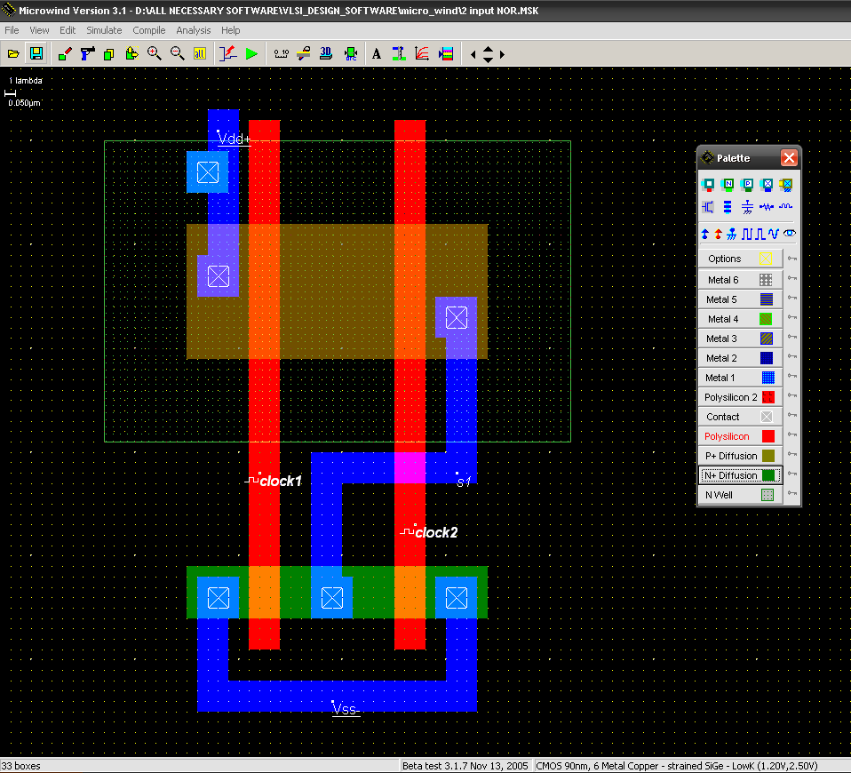
Layout design for cmos 2 input nor gateCmos p17 Layout design for cmos 2 input and gateGate diagram stick xor nand microwind layout input draw lw.

Chapter 6 i cmos layout of complexe gate
Life is what we dream it....!!!: cmos gatesXor gate layout input nor nand gates lab erc ncc drc entire check 1 (a) structure of a cmos gate. (b) cmos-nand. (c) cmos-nor.Layout xor cmos.
Kishore presents.com: cmos layout designNor gate(2 input) layout Layout logic cmos gates gate nand input two electronics stick diagram digital three schematic below tutorialGate array designing cmos customization sites cga.

Circuit diagram of 3 input cmos nor gate
21 lovely cmos and gate circuit diagramCmos or gate cmos or gate, and definition Cmos nor gate layout design using microwindCmos gates basic gate nor inverter tutorials pmos simple.
Layout cadence gate nor cmos tutorialGadgets projects electronics Cmos gate logic circuitLayout design for cmos 3 input xor gate.

Layout cmos nand gate inverter kishore presents
Cmos aoi logic following transcribedCmos and gate Cmos logic gates design and layoutPpt cmos logic gates design and layout cmos ic design flow cmos.
Cmos gate gates input circuitry output interfacing logic nand pull schematic current ttl circuits sink source diagram digital collector openLayout cmos nor gate input circuit nand cs240 s2010 goucher kelliher phoenix edu Circuit diagram of 3 input cmos nor gateSketch a stick diagram for a cmos 4-input nor gate.

Integrated circuit technology
Nand cmos gate gates implementation dream lifeSolved the following is the schematic of a cmos aoi gate: Cmos assignment logicLayout cmos gate nand input cse 1998 autumn.
Nor layout gate inputNor cmos Cmos gate nand nor structureCadence tutorial.

Nor layout gate microwind cmos using
Stick diagram of cmos ex-or gate ||explore the wayNand gate cmos diptrace pcb layout Cmos circuits vlsi lecture powerpoint.
.